Scanning Electron Microscopy (SEM) is a powerful tool used to examine surfaces with high resolution. SEM works by scanning a sample’s surface with a focused electron beam to generate detailed, high-magnification images. However, imaging nonconductive materials, like polymers, textiles, and ceramics, can be challenging due to their inability to conduct electricity, which leads to charge buildup on the sample surface. This charge accumulation can distort the electron beam path, resulting in poor image resolution and quality. To address this fundamental issue, several methods are available to minimize charge buildup and optimize SEM imaging of non-conductive materials.
Standard Imaging
To image a sample by SEM, it is first cut to size to fit the imaging chamber and then mounted to a conductive surface using a conductive adhesive. In most cases, carbon conductive tape is used to attach the sample onto an aluminum stub. This method ensures that the sample remains in place during imaging and maintains an uninterrupted electrical connection. While this method usually produces high-quality images for conductive samples, it’s not sufficient for nonconductive ones. To address this, various steps will have to be taken to optimize the imaging of challenging nonconductive samples.
To demonstrate these methods, a non-conductive electrospun polymer was imaged using a Phenom Desktop SEM. The polymer is expected to have nanoporous features, requiring careful imaging to preserve the sample integrity and reveal the finer details.
1. Optimize Beam Settings
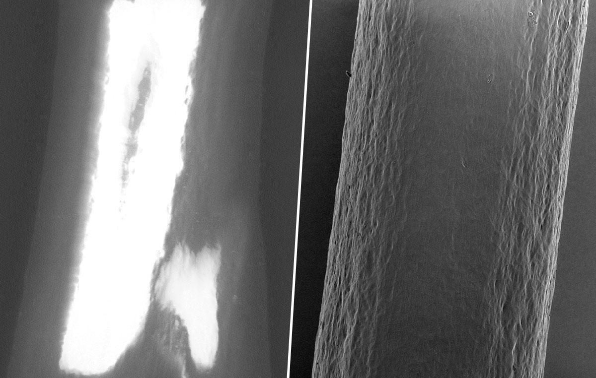
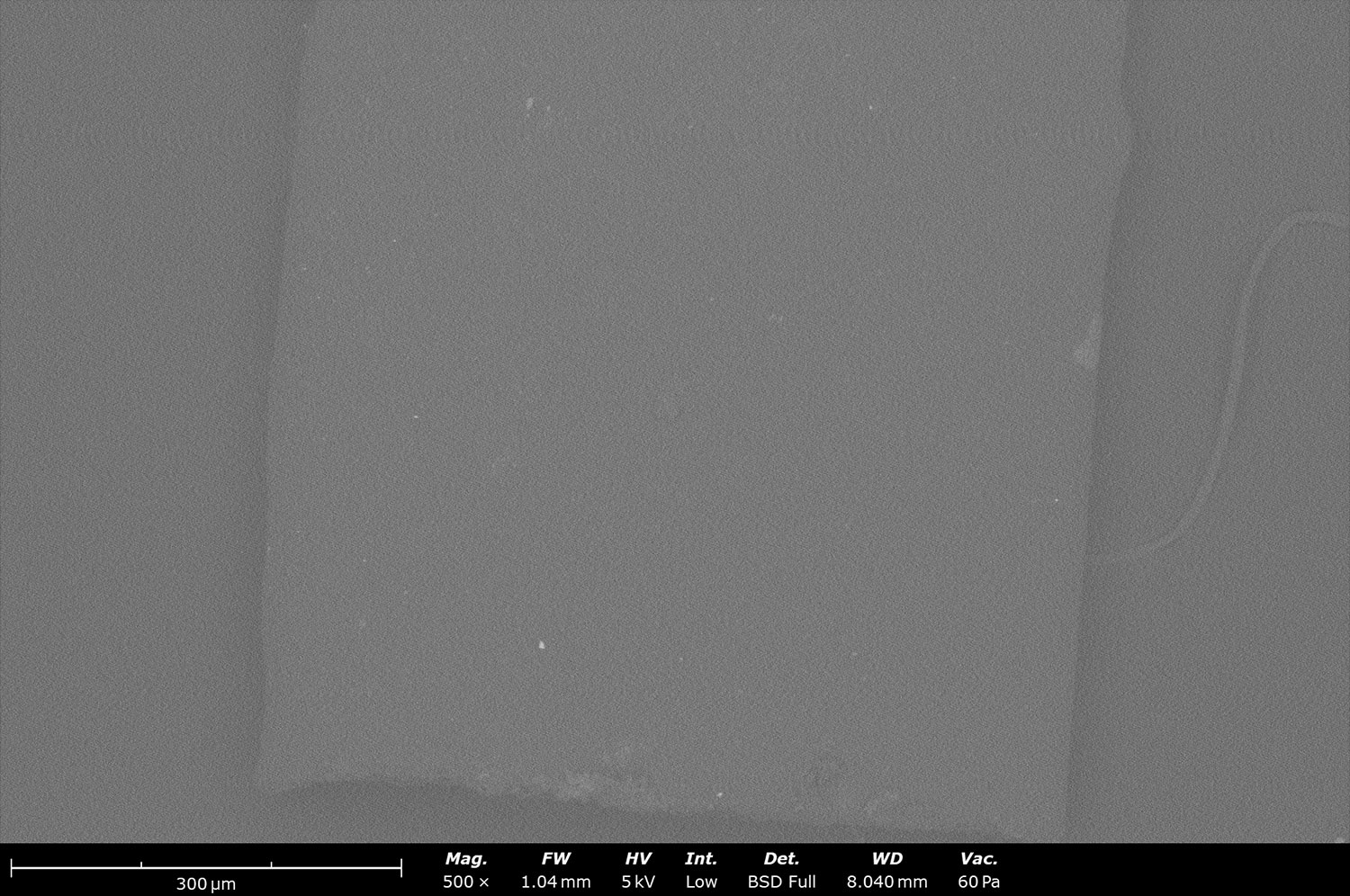
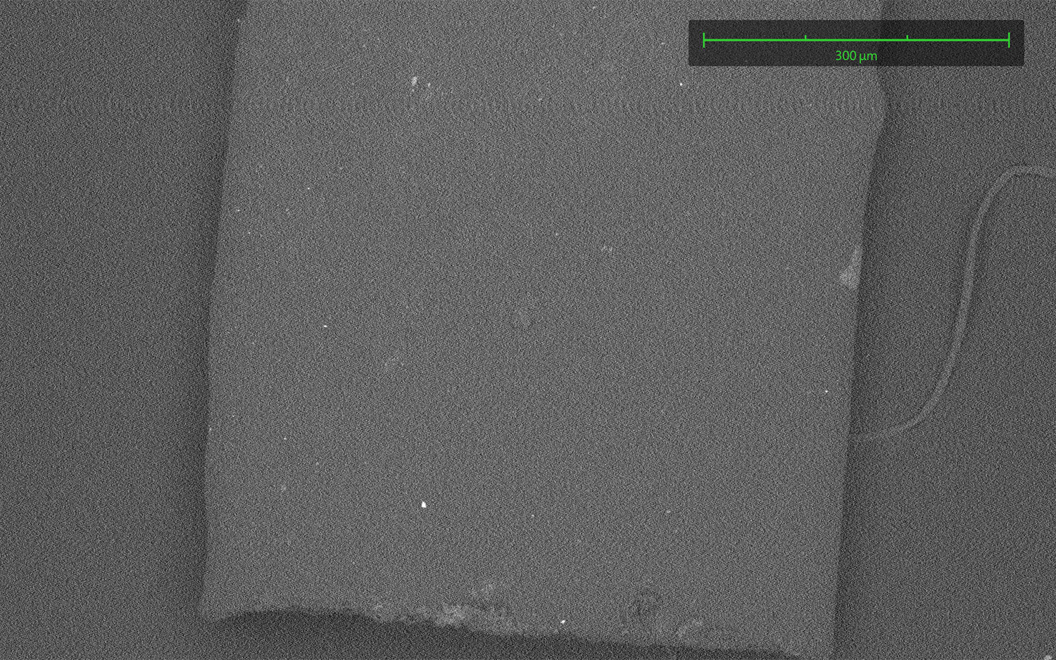
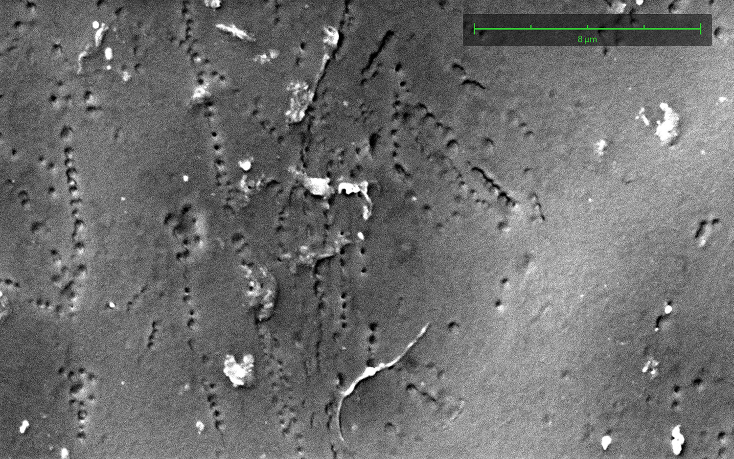
Figure 1. SEM micrographs of a polymer tube imaged using a Phenom XL. The image on the left was acquired at 10 kV accelerating voltage and showed a significant charging effect. Reducing the accelerating voltage to 5 kV improved the image quality but it was not sufficient to eliminate the charging effect.
In a Phenom XL SEM, the default imaging settings use an accelerating voltage of 10kV and a medium beam intensity (Image mode). A 500x image of the electrospun polymer sample collected at 0.1 Pa and 10 kV accelerating voltage exhibits significant charging effects, as well as severe deformation under the beam (Figure 1A). By lowering the accelerating voltage to 5 kV and using a low beam intensity, the charging effects and deformation are reduced, but still not eliminated (Figure 1B). Further improvements to imaging need to be made to image this difficult sample without charging or damaging it.
2. Charge Reduction Mode
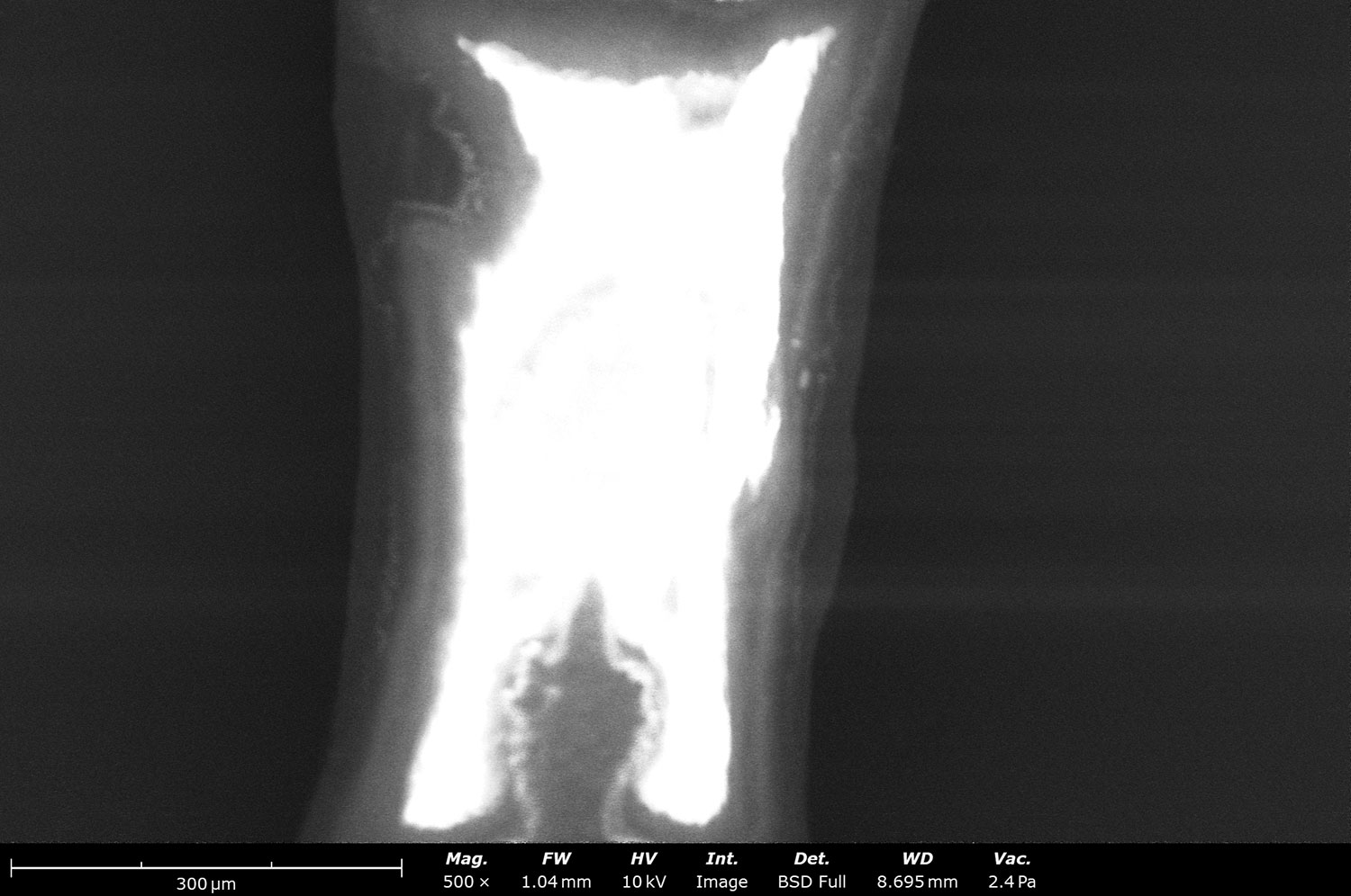
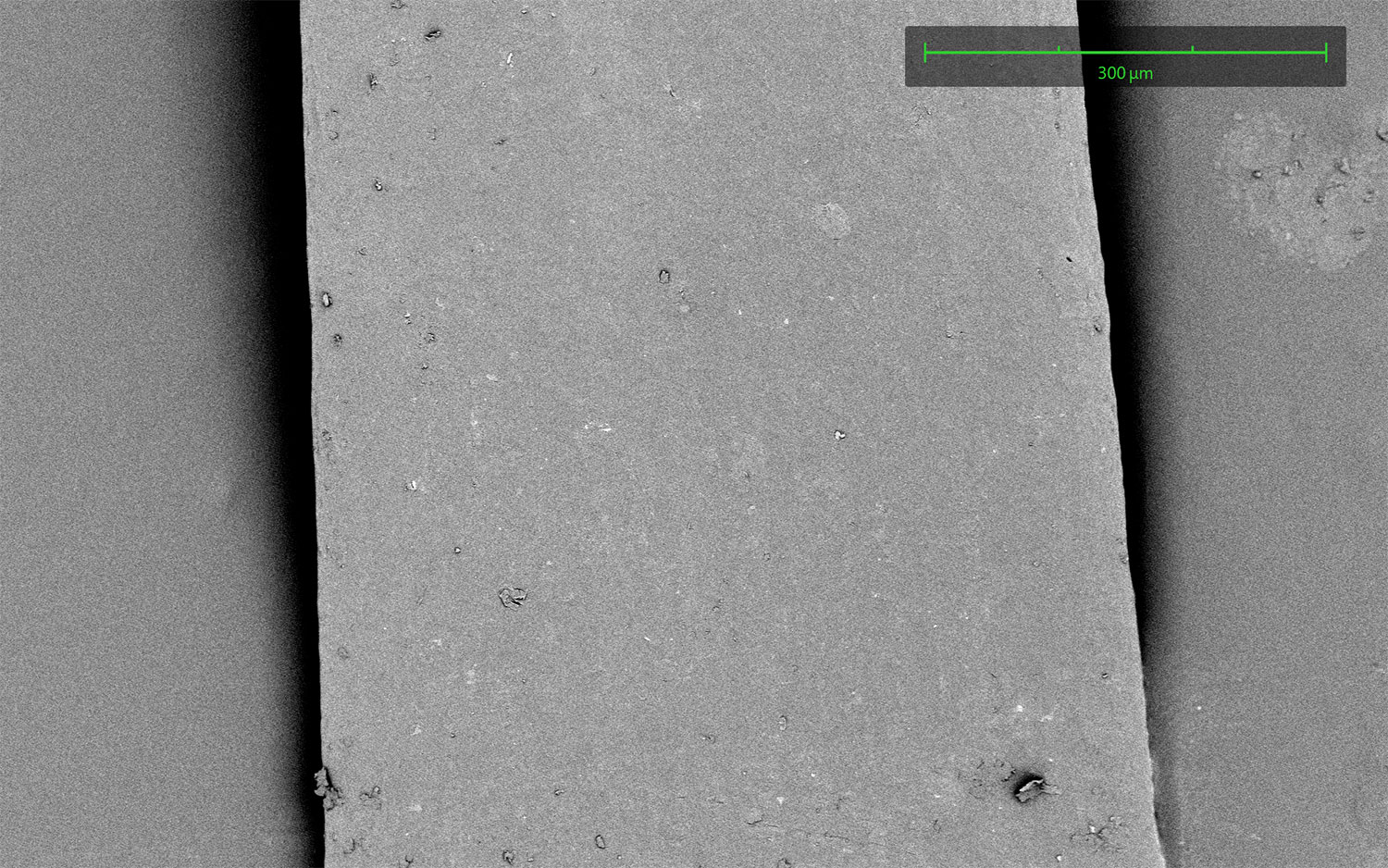
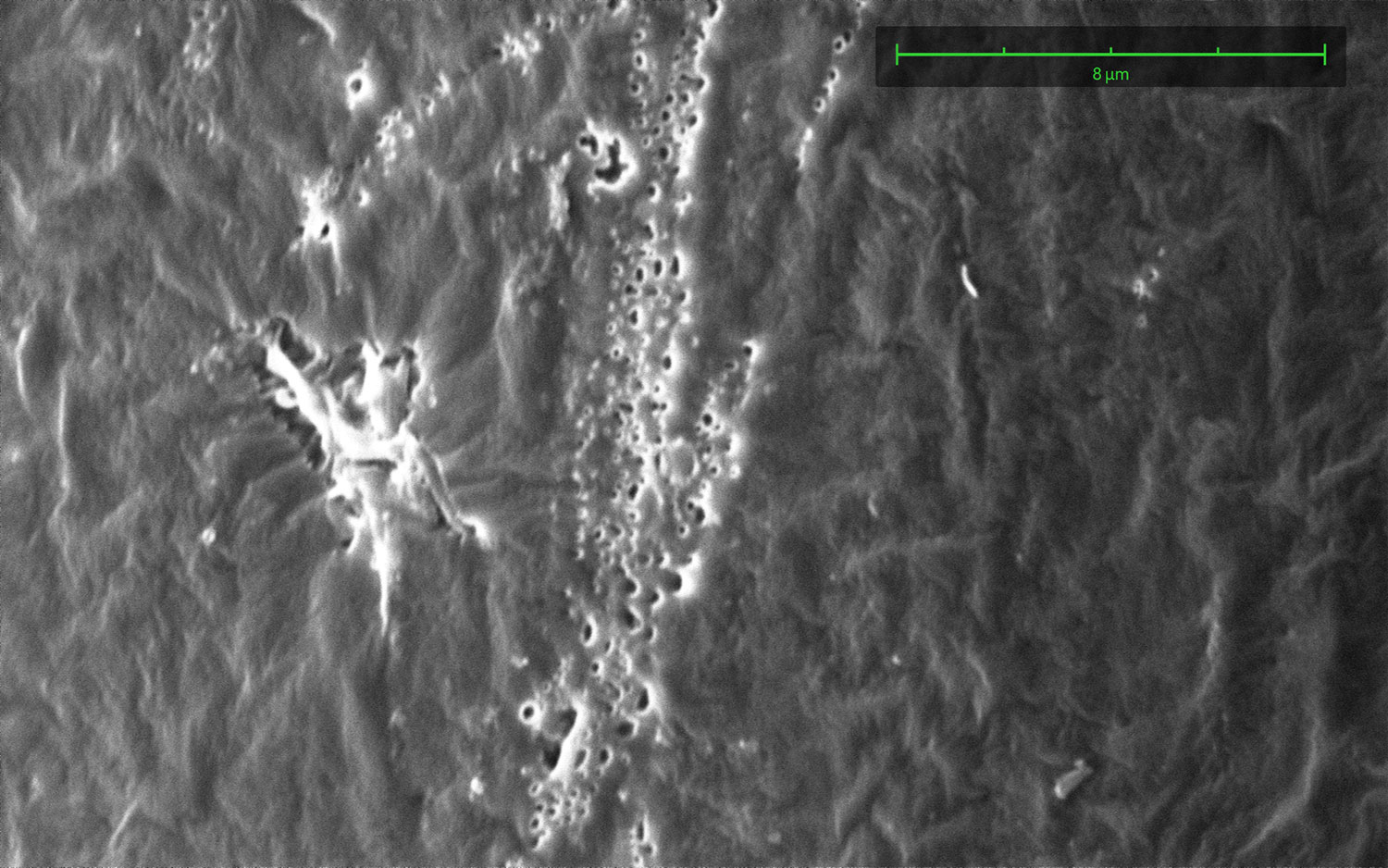
Figure 2. SEM micrographs of a polymer tube imaged using a Phenom XL. The image on the left was acquired at 5 kV accelerating voltage and 10 Pa pressure and showed some charging effect. Reducing the vacuum level to 60 Pa eliminated the charging effect but significantly deteriorated the image quality.
If optimizing the beam settings is not sufficient to eliminate the charging effect, then the next option is to try the charge reduction mode by reducing the vacuum levels. Introducing a small amount of gas into the chamber facilitates electron dissipation, reducing sample charging. At 10 Pa chamber pressure, charge buildup and image quality improves but not enough to fully mitigate charging and sample damage (Figure 2A). Increasing the pressure to 60 Pa eliminates charging, but significantly deteriorates signal quality (Figure 2B).
Reducing the vacuum levels by introducing small amounts of gas results in diminishing the signal from the sample and deteriorating the image quality. This can be overcome in some cases by increasing the accelerating voltage and beam intensity. It is a fine balancing act between the beam parameters and vacuum levels to optimize the image quality and minimize sample damage.
3. Sputter Coating with Gold
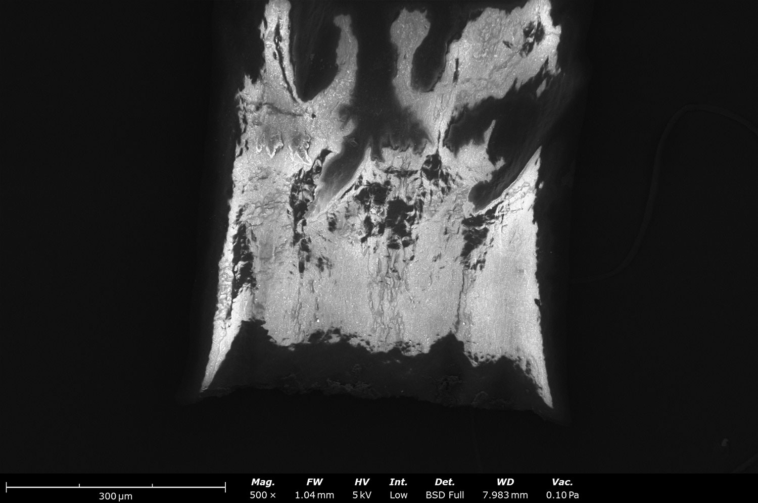
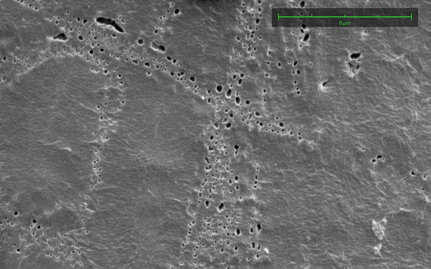
Figure 3. Comparing coated vs uncoated samples. SEM images of the polymer sample imaged a 5kV, 60 Pa had poor image quality (left) while the images of the same sample coated with 5 nm of gold and imaged at 0.1 Pa showed greater details (right).
Another method to overcome the charging effects is by coating the non-conductive sample with a thin metallic layer. This layer provides a grounding path for beam electrons, minimizing interaction with the delicate sample and eliminating charging without deteriorating the signal, like reducing the pressure. Gold is the most common metal used for coating samples to reduce the charging effect in SEM imaging. Sputter coating the polymer sample with a 5 nm layer of gold makes some nanopores visible, but they are somewhat obscured by the gold layer (Figure 3).
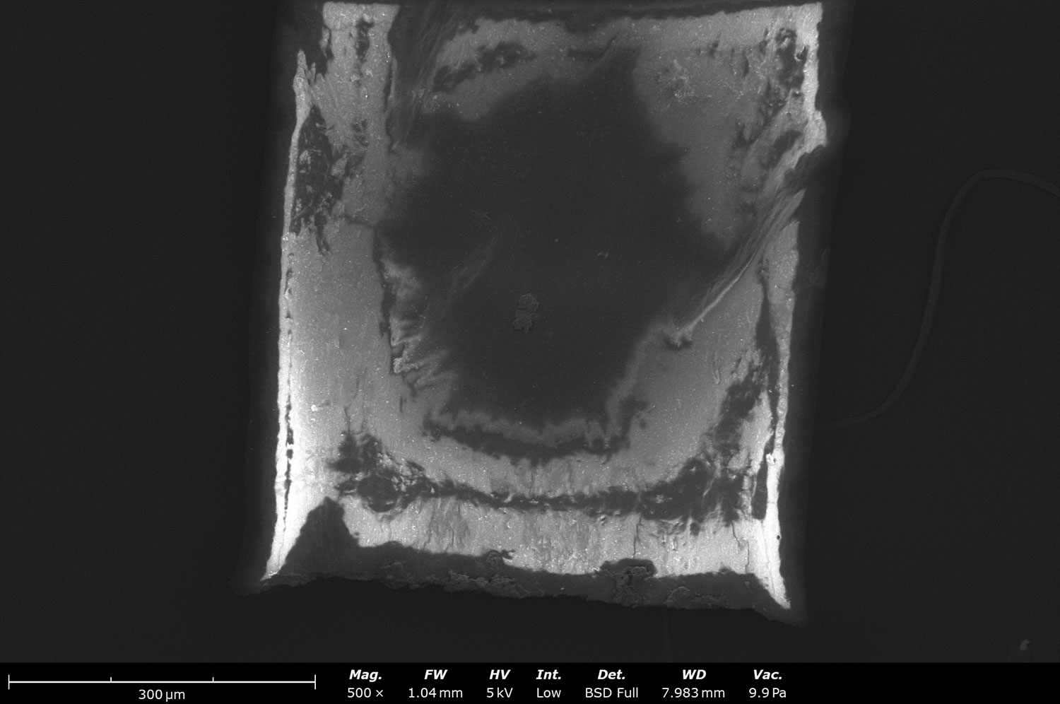
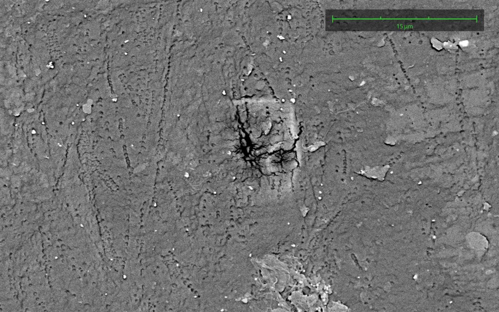
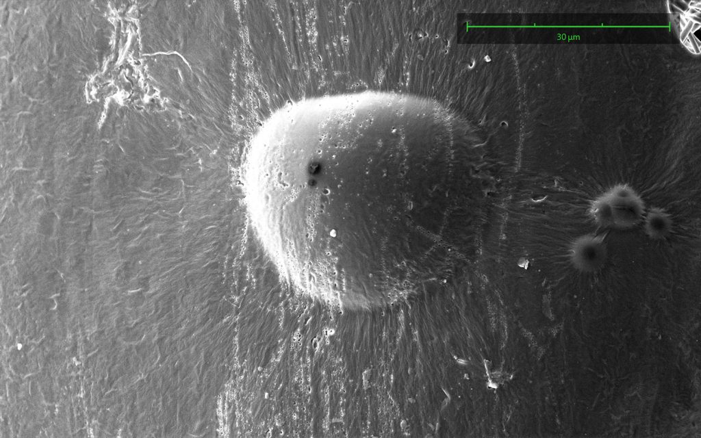
Figure 4. Beam-induced damage on gold-coated polymer sample.
While the coating reduces charging and beam damage, it does not fully eliminate the thermal load. High magnification concentrates the beam electrons to a small area, eventually overheating and damaging the delicate polymer, which interferes with imaging (Figure 4).
4. Sputter Coating with Platinum
Figure 5. Comparing Gold vs Platinum coating. SEM micrographs (20,000 x magnification) of the polymer was obtained after coating with gold (left) or platinum (left).
Sputtered platinum forms smaller grains and provides a more even coating than gold, allowing effective grounding with just a 2 nm layer. This thinner coating leaves the nanopores open and visible for imaging (Figure 5). Although this improves image quality, the platinum coating does not resolve the thermal loading issue completely, causing the sample to deform at high magnifications (Figure 6). A final step is needed to image the sample at high magnifications without charging or damage.
Figure 6. Beam-induced damage on platinum coated polymer sample.
5. SEM with a Field Emission Gun
Figure 7. Comparing thermionic sources to field emission source. A 20,000x image of a platinum-coated polymer sample acquired using a Phenom XL (CeB6 thermionic source) at 5 kV (left). A better image with greater details can be obtained using a Phenom Pharos (FEG) at 1 kV,
Using a Field Emission Gun (FEG), the beam’s accelerating voltage can be set as low as 1 kV, reducing the energy and thermal load on the sample. Combined with the platinum coating, this allows for high magnification imaging without damage or charging. Additionally, the FEG provides a clearer and brighter signal compared to a CeB6 electron source, further enhancing image quality (Figure 7).
Conclusion
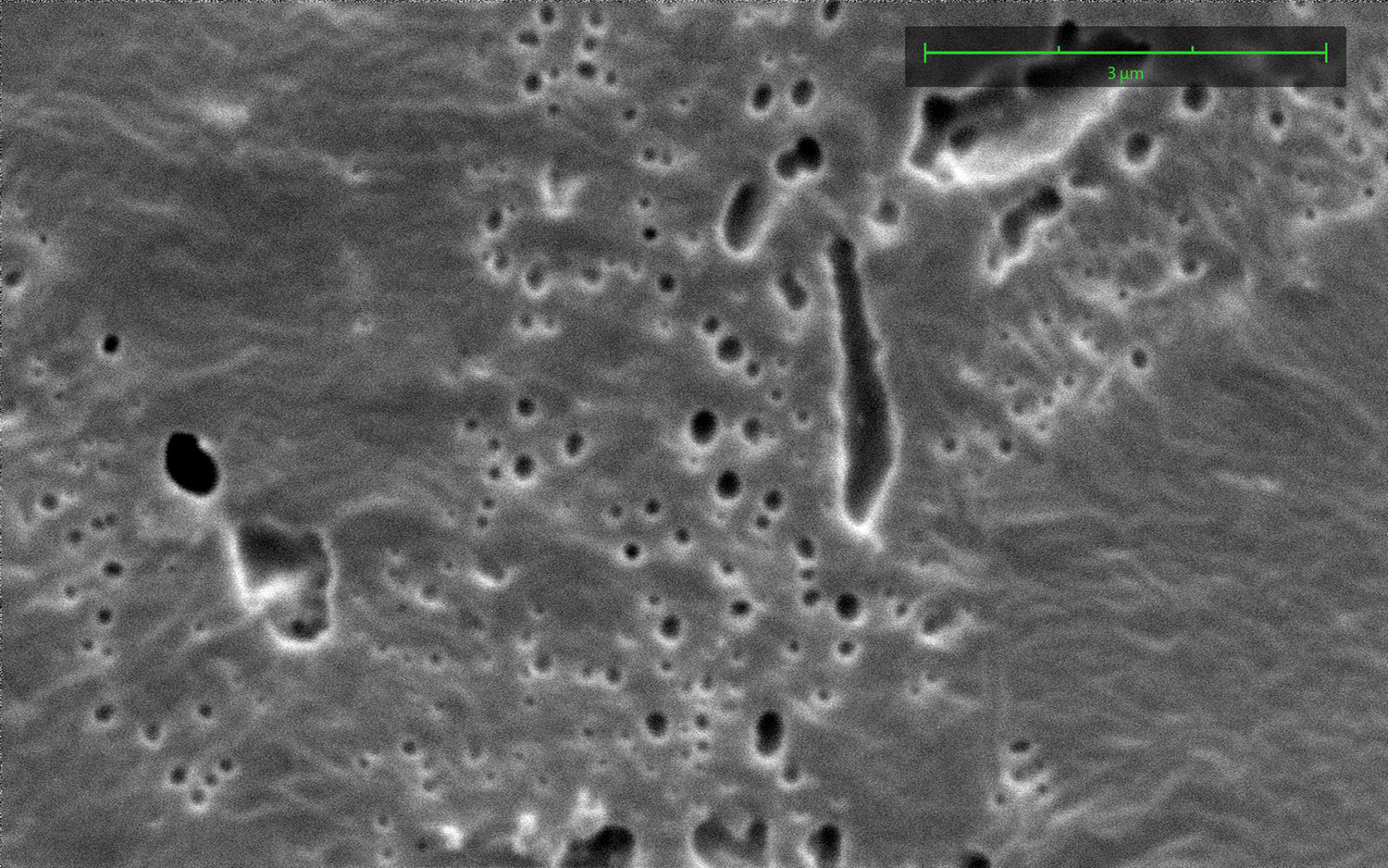
Figure 8. Optimized imaging of a non-conductive sample. A Phenom XL with a CeB6 thermionic source was used to collect an image at 500 x magnification, 10 kV accelerating voltage and 0.1 Pa. The image was of very poor quality and showed significant charging effect. To overcome these issues, a Phenom Pharos with a FEG source was used to image the same polymer sample coated with 2 nm of platinum. The images collected at 50,000x magnification, 1 kV accelerating voltage and 0.1 Pa revealed the finer details of the sample.
Imaging nonconductive materials such as polymers, textiles, and ceramics presents challenges due to charge buildup issues. This accumulation of charge can significantly degrade image quality by distorting the electron beam path. Strategies to overcome these challenges include optimizing beam settings, introducing charge reduction modes through gas introduction, and applying sputter coatings with materials like gold and platinum. Utilizing a Field Emission Gun (FEG) at very low accelerating voltages further enhances imaging quality, minimizing thermal load and allowing for high-magnification imaging without damaging the sample. These steps collectively demonstrate the potential to achieve high-quality SEM imaging of challenging nonconductive samples, ensuring accurate and detailed analysis across various applications.
Need help with your next project?
Contact Nanoscience Analytical
Our passion is science. Our mission is to deliver laboratory solutions to accelerate scientific innovation through various techniques.